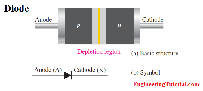
A diode is made from a small piece of semiconductor material, usually silicon, in which half is doped as a p region and half is doped as an n region with a pn junction and depletion region in between. The p region is called the anode and is connected to a conductive terminal. The n region is called the cathode and is connected to a second conductive terminal. The basic diode structure and schematic symbol are shown below
Forward Bias
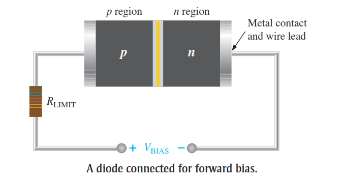
To bias a diode, we apply a dc voltage across it. Forward bias is the condition that allows current through the pn junction. Below Figure shows a dc voltage source connected by conductive material (contacts and wire) across a diode in the direction to produce forward bias. This external bias voltage is designated as Vbias. The resistor limits the forward current to a value that will not damage the diode. Notice that the negative side of Vbias is connected to the n region of the diode and the positive side is connected to the p region. This is one requirement for forward bias. A second requirement is that the bias voltage, Vbias, must be greater than the barrier potential of diode.
A fundamental picture of what happens when a diode is forward-biased is shown in Below Figure. Because like charges repel, the negative side of the bias-voltage source “pushes” the free electrons, which are the majority carriers in the n region, toward the pn junction. This flow of free electrons is called electron current. The negative side of the source also provides a continuous flow of electrons through the external connection (conductor) and into the n region as shown.
The bias-voltage source imparts sufficient energy to the free electrons for them to over-come the barrier potential of the depletion region and move on through into the p region. Once in the p region, these conduction electrons have lost enough energy to immediately combine with holes in the valence band.
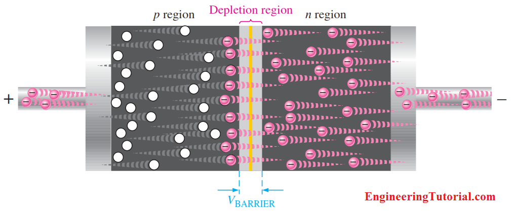
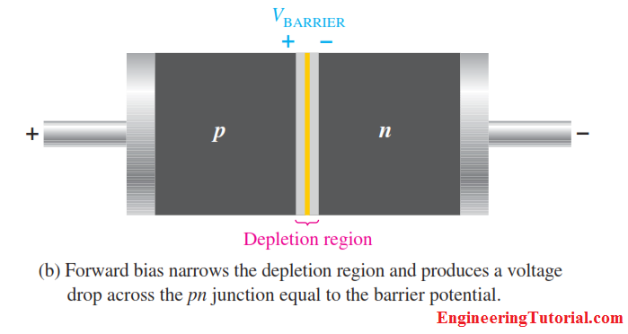
Fig: A forward-biased diode showing the flow of majority carriers and the voltage due to the barrier potential across the depletion region.
Now, the electrons are in the valence band in the p region, simply because they have lost too much energy overcoming the barrier potential to remain in the conduction band. Since unlike charges attract, the positive side of the bias-voltage source attracts the valence electrons toward the left end of the p region. The holes in the p region provide the medium or “pathway” for these valence electrons to move through the p region. The valence electrons move from one hole to the next toward the left. The holes, which are the majority carriers in the p region, effectively (not actually) move to the right toward the junction, as you can see in Above Figure. This effective flow of holes is the hole current. You can also view the hole current as being created by the flow of valence electrons through the p region, with the holes providing the only means for these electrons to flow.
As the electrons flow out of the p region through the external connection (conductor) and to the positive side of the bias-voltage source, they leave holes behind in the p region; at the same time, these electrons become conduction electrons in the metal conductor. Recall that the conduction band in a conductor overlaps the valence band so that it takes much less energy for an electron to be a free electron in a conductor than in a semiconductor and that metallic conductors do not have holes in their structure. There is a continuous availability of holes effectively moving toward the pn junction to combine with the continuous stream of electrons as they come across the junction into the p region.
The Effect of Forward Bias on the Depletion Region
As more electrons flow into the depletion region, the number of positive ions is reduced. As more holes effectively flow into the depletion region on the other side of the pn junction, the number of negative ions is reduced. This reduction in positive and negative ions during forward bias causes the depletion region to narrow, as indicated in Below Figure.
Fig : The depletion region narrows and a voltage drop is produced across the pn junction when the diode is forward-biased.
The Effect of the Barrier Potential During Forward Bias
The electric field between the positive and negative ions in the depletion region on either side of the junction creates an “energy hill” that prevents free electrons from diffusing across the junction at equilibrium. This is known as the barrier potential.
When forward bias is applied, the free electrons are provided with enough energy from the bias-voltage source to overcome the barrier potential and effectively “climb the energy hill” and cross the depletion region. The energy that the electrons require in order to pass through the depletion region is equal to the barrier potential. In other words, the electrons give up an amount of energy equivalent to the barrier potential when they cross the depletion region. This energy loss results in a voltage drop across the pn junction equal to the barrier potential (0.7 V), as indicated in Above Figure (b). An additional small voltage drop occurs across the p and n regions due to the internal resistance of the material. For doped semiconductive material, this resistance, called the dynamic resistance, is very small and can usually be neglected.
Reverse Bias
Reverse bias is the condition that essentially prevents current through the diode. Below Figure shows a dc voltage source connected across a diode in the direction to produce reverse bias. This external bias voltage is designated as VBIAS just as it was for forward bias. Notice that the positive side of VBIAS is connected to the n region of the diode and the negative side is connected to the p region. Also note that the depletion region is shown much wider than in forward bias or equilibrium.
An illustration of what happens when a diode is reverse-biased is shown in Below Figure. Because unlike charges attract, the positive side of the bias-voltage source “pulls” the free electrons, which are the majority carriers in the n region, away from the pn junction. As the electrons flow toward the positive side of the voltage source, additional positive ions are created. This results in a widening of the depletion region and a depletion of majority carriers.
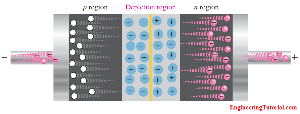
Fig : The diode during the short transition time immediately after reverse-bias voltage is applied.
In the p region, electrons from the negative side of the voltage source enter as valence electrons and move from hole to hole toward the depletion region where they create additional negative ions. This results in a widening of the depletion region and a depletion of majority carriers. The flow of valence electrons can be viewed as holes being “pulled” to ward the positive side.
The initial flow of charge carriers is transitional and lasts for only a very short time after the reverse-bias voltage is applied. As the depletion region widens, the availability of majority carriers decreases. As more of the n and p regions become depleted of majority carriers, the electric field between the positive and negative ions increases in strength until the potential across the depletion region equals the bias voltage, VBIAS. At this point, the transition current essentially ceases except for a very small reverse current that can usually be neglected.
Reverse Current
The extremely small current that exists in reverse bias after the transition current dies out is caused by the minority carriers in the n and p regions that are produced by thermally generated electron-hole pairs. The small number of free minority electrons in the p region are “pushed” toward the pn junction by the negative bias voltage.
When these electrons reach the wide depletion region, they “fall down the energy hill” and combine with the minority holes in the n region as valence electrons and flow toward the positive bias voltage, creating a small hole current. The conduction band in the p region is at a higher energy level than the conduction band in the n region. Therefore, the minority electrons easily pass through the depletion region because they require no additional energy. Reverse current is illustrated in Below Figure.
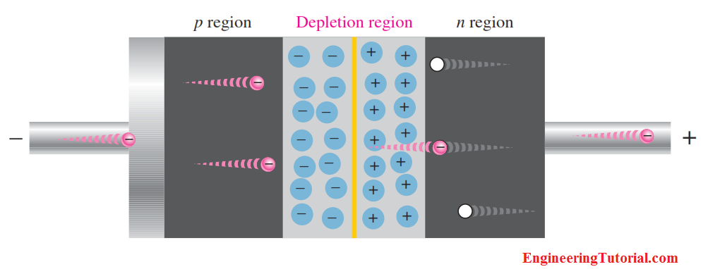
Fig : The extremely small reverse current in a reverse-biased diode is due to the minority carriers from thermally generated electron-hole pairs.
Reverse Breakdown
Normally, the reverse current is so small that it can be neglected. However, if the external reverse-bias voltage is increased to a value called the breakdown voltage, the reverse current will drastically increase.
This is what happens. The high reverse-bias voltage imparts energy to the free minority electrons so that as they speed through the p region, they collide with atoms with enough energy to knock valence electrons out of orbit and into the conduction band. The newly created conduction electrons are also high in energy and repeat the process. If one electron knocks only two others out of their valence orbit during its travel through the p region, the numbers quickly multiply. As these high-energy electrons go through the depletion region, they have enough energy to go through the n region as conduction electrons, rather than combining with holes.
The multiplication of conduction electrons just discussed is known as the avalanche effect, and reverse current can increase dramatically if steps are not taken to limit the current. When the reverse current is not limited, the resulting heating will permanently damage the diode. Most diodes are not operated in reverse breakdown, but if the current is limited (by adding a series-limiting resistor for example), there is no permanent damage to the diode.