What is the effect of negative feedback on voltage gain, BW, Noise, nonlinear distortion, Ri, Ro of a voltage amplifier?
The voltage gain, bandwidth, noise, nonlinear distortion, input resistance, output resistance are
Voltage gain with feedback = Voltage gain without feedback* desensitivity factor (since desensitivity factor << 1 in negative feedback, hence Voltage gain without feedback < gain without feedback).
Band width with feedback = Band width without feedback/ desensitivity factor (since desensitivity factor << 1 in negative feedback, hence Band width without feedback > Band width without feedback).
Noise with feedback = Noise without feedback* desensitivity factor (since desensitivity factor << 1 in negative feedback, hence Noise without feedback > Noise without feedback).
Non linear distortion with feedback = Non linear distortion without feedback* desensitivity factor (since desensitivity factor << 1 in negative feedback, hence Non linear distortion without feedback > Non linear distortion without feedback).
Non linear distortion with feedback = Non linear distortion without feedback* desensitivity factor (since desensitivity factor << 1 in negative feedback, hence Non linear distortion without feedback > Non linear distortion without feedback).
Input resistance with feedback = Input resistance without feedback/ desensitivity factor (since desensitivity factor << 1 in negative feedback, hence Input resistance without feedback > Input resistance without feedback).
Output resistance with feedback = Output resistance without feedback* desensitivity factor (since desensitivity factor << 1 in negative feedback, hence Output resistance without feedback > Output resistance without feedback)
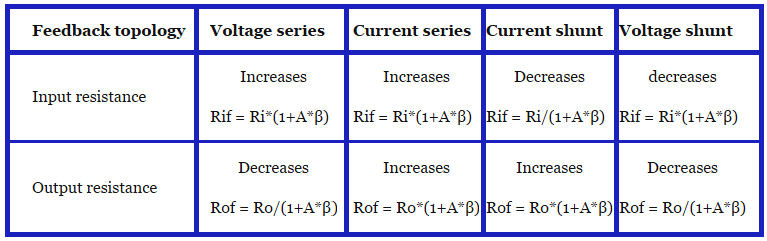
What are the different types of feedback topologies?
There are four different types of feedback topologies based on type of output signal and feedback signal (voltage or current signal). Voltage feedback is taken in series with the load and current feedback is taken in shunt with the load. They are
a)Voltage-series: Output signal is voltage signal, feedback signal is voltage signal. Also called as series-series feedback. It is employed in voltage amplifiers.
b)Current series: Output signal is current signal, feedback signal is voltage signal. Also called as shunt-series feedback. It is employed in Transconductance amplifiers.
c)Current shunt: Output signal is current signal, feedback signal is current signal. Also called as shunt-shunt feedback. It is employed in current amplifiers.
d)Voltage shunt: Output signal is voltage signal, feedback signal is current signal. Also called as shunt-shunt feedback. It is employed in current amplifiers.
The first word indicates the type of output signal and the second word indicates the manner in which feedback signal is taken whether it is taken in series or shunt with the load.
What is the effect of each feedback network topologies on input and output resistance?
What is a nyquist criterion to differentiate the feedback in amplifiers?
If the nyquist plot of amplifiers encircles (-1, 0) point in nyquist domain, the amplifier is unstable and has positive feedback.
If the nyquist plot of amplifiers does not encircle (-1, 0) point in nyquist domain, the amplifier is stable and has negative feedback.
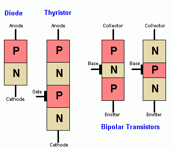
What are CS, CD, and CG amplifiers?
Common Source amplifier is on in which the Source terminal is common to both input and output circuit.
Common Drain amplifier is on in which the Drain terminal is common to both input and output circuit.
Common Gate amplifier is on in which the Gate terminal is common to both input and output circuit.
Give expressions for Ri, Ro, Voltage gain of CS, CD, CG?
The following equations are provided for MOSFET’s with voltage divider bias arrangement having Rg1 and Rg2 as biasing resistors at the gate terminal and constant current source at the source terminal.
| Amplifier/Parameter | Input resistance | output resistance | Voltage gain |
| Common Source amplifier | Rg | ro//Rd | -gm*(ro//Rd//Rl) |
| Common Drain amplifier(Neglecting ro) | Rg | Rd | -gm*(Rd//Rl) |
| Common Gate amplifier(Neglecting ro) | 1/gm | Rd | gm*(Rd//Rl) |
Where Rg = Rg1//Rg2, gm is Transconductance, Rd is the resistance at the drain terminal.
Define conduction angle in power amplifier?
The time during which the transistor conducts i.e. (the collector current is non zero) when an input sinusoidal signal is applied in a power amplifier is defined as Conduction angle.
What are the types of distortions encountered in amplifiers?
There are mainly three types of distortions encountered in amplifiers. They are
a) Non linear distortion: It occurs due to non dynamic curve of input output characteristics in amplifiers. New frequencies appear in the output due to non linear distortion. It is often encountered in large signal amplifiers.
b) Frequency distortion: This type of distortion occurs when the signal components of different frequencies are amplified differently.
c) Phase distortion: Phase distortion occurs due to unequal phase shift of signals of different frequencies.
Frequency and phase distortion occurs when the signal frequencies lie outside the band width of amplifier.
What are types of power amplifier based on conduction angle?
There are mainly four types of amplifiers based on conduction angle. They are
a) Class A amplifiers
b) Class B amplifiers
c) Class AB amplifiers
d) Class C amplifiers
What is class A, Class B, Class AB, Class C amplifiers?
Class A amplifier: In class-A amplifiers the collector is biased at a value greater than the amplitude of AC signal current. Hence the conduction angle is 360 Degrees i.e. the Class A stage conducts for the entire cycle for the input signal.
Class B amplifier: Class B amplifiers are biased at zero DC bias collector current. Hence it conducts only for half of the input signal cycle, so the conduction angle for class B amplifier is 180 Degrees.
Class AB amplifier: In class AB amplifiers the biasing current is non zero but much smaller than the peak current of the sine wave signal. As a result the transistor conducts for interval slightly greater than half a cycle. The conduction angle is slightly greater than 180 Degrees.
Class C amplifier: In class C amplifier the transistor conducts for an interval less than the half cycle. Hence the conduction angle is less than 180 Degrees.
What is push-pull amplifier?
A push pull amplifier is a special type of arrangement used in class B amplifiers where the active device pair push (supply) current and pull (absorb) current from load. Push pull amplifiers are more efficient than the single ended power amplifiers. Because of the symmetric construction of two sides of the amplifier the even harmonics are cancelled and output signal distortion can be minimized. Another advantage of the push pull amplifier is the effect of ripple voltage that may be contained in the power supply is balanced out. The main disadvantages of the push pull amplifier are the need for two identical transistors and the requirement of bulky and costly coupling transformers used for phase splitting.
What is complementary push-pull amplifier?
Complementary Push-pull amplifiers use two “complementary” or matching transistors, one being an NPN-type and the other being a PNP-type with both power transistors receiving the same input signal together that is equal in magnitude, but in opposite phase to each other. This results in one transistor only amplifying one half of the input waveform cycle while the other transistor amplifies the other half of the input waveform cycle with the resulting “two-halves” being put back together again at the output terminal. In complementary push pull amplifier neither an input nor an output transformer is needed. The main difficulty with this circuit is the if there is unbalance in the characteristic f the two transistors considerable distortion will be introduced.
What is non-linear distortion in power amp?
Non-linear distortion occurs due to non dynamic curve of input output characteristics in amplifiers because of which the output waveform differs from the input. Active devices such as transistors, FET’s have linear input output characteristic for small signal variations around the Q-point. But in case of large signal variations around the Q-point considerable non linearity is introduced in the output.
Consider a power amplifier which is given a input of A*sin (w*t), the output is in the form of A1*sin (w*t) + A2*sin (2*w*t)+A3*sin(3*w*t)+……… The ratio of |A2/A1| is called as second harmonic distortion. Similarly |A3/A1| is called third harmonic distortion and so on. The total harmonic distortion is defined as D = (D1^2+D2^2+D3^2+…….)^(1/2). Therefore the total power is given as Pt= P(1+D^2) where P is the power delivered at fundamental frequency.
If the input consists of two different frequencies w1 and w2 then the inter modulation frequencies (sum or difference frequencies) w1+w2 and w1-w2 are introduced into the output
What is tuned amplifier? Where it is used?
Tuned amplifier is one in which a tuned circuit is introduced in to the output circuit which draws maximum power output only for a specified range of frequencies. Example of a tuned amplifier is shown below

tuned amplifier
The tuned amplifier shown in the figure will deliver maximum power only in the bandwidth of LC resonant circuit. Tuned amplifiers are used in video and radio frequency applications. They are used as frequency selective amplifiers in multi communication channels such as radio and TV broadcasting through wireless medium where each station is assigned a frequency band. They are used in RF/Wireless transceivers and intermediate stages of IF amplifiers.
What are the Types of amplifiers?
There are four types of amplifiers based on input signal fed to it and the output signal extracted from it. They are
- Voltage amplifier
- Current amplifier
- Trans conductance amplifier
- Trans resistance amplifier
Define Transconductance, Transresistance, voltage gain, current gain?
Voltage gain of an amplifier is defined as ratio of output voltage to input voltage fed to amplifier. It is unit less and is denoted by Av.
Voltage gain Av = Vo/Vi
Current gain of an amplifier is defined as ratio of output current to input current fed to amplifier. It is unit less and is denoted by Av.
Voltage gain Ai = Io/Ii
Transconductance of an amplifier is defined as ratio of output current to input voltage fed to amplifier. It is specified in units of mhos (or) Siemens and is denoted by Rt.
Transconductance Rt = Vo/ Ii
Trans-resistance of an amplifier is defined as ratio of output voltage to input current fed to amplifier. It is specified in units of ohms and is denoted by Rt.
Trans-resistance Rt = Vo/ Ii
What are the Ideal input and output resistances of various amplifiers?
| Parameter/Type of amplifier | Voltage amplifier | Current amplifier |
Transconductance amplifier |
Transresistance amplifier |
|
| Input resistance | Infinite | Zero | Infinite | Zero | |
| Output resistance | Zero | Infinite | Infinite | Zero |
What is an Audio amplifier?
Audio amplifiers are electronic power amplifiers used to amplify low intensity audio signals to a level suitable to drive loud speakers. The audio frequencies are in the range 20 Hz to 20,000 Hz. Normally Class AB power amplifiers are used to do audio amplification. Phase distortion will not create much problem in audio amplifiers.
What is a Video amplifier?
These amplifiers are use to amplify video signals. These amplifiers have varying bandwidths based on the type of filter used at each point. Typically a low-pass amplifier will be having a bandwidth in the range from 2 to 10 MHz. Some of the applications are in television receivers, cathode-ray-tube computer terminals, and pulse amplifiers. The phase distortion is of prime concern in video amplifiers; hence extra elements are added to nullify distortion.
What is Power amplifier?
A power amplifier stage is an amplifier optimized to deliver high output power. Special attention has to be paid in designing such amplifiers as the power dissipation across the junction raises its temperature and eventually destroys it. In practice we can observe that the power transistors are bulky in nature to handle high powers as high surface area leads to high heat removing capacity.
Also Read: Basics of Amplifiers Q&A