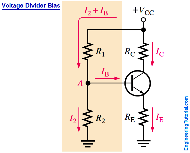
A method of biasing a transistor for linear operation using a single-source resistive voltage divider. This is the most widely used biasing method.

Up to this point a separate dc source, VBB, was used to bias the base-emitter junction because it could be varied independently of VCC and it helped to illustrate transistor operation. A more practical bias method is to use VCC as the single bias source, as shown in the above Figure.
To simplify the schematic, the battery symbol is omitted and replaced by a line termination circle with a voltage indicator (VCC) as shown. A dc bias voltage at the base of the transistor can be developed by a resistive voltage-divider that consists of R1 and R2, as shown in Figure. VCC is the dc collector supply voltage. Two current paths are between point A and ground: one through R2 and the other through the base-emitter junction of the transistor and RE. Generally, voltage-divider bias circuits are designed so that the base current is much smaller than the current (I2) through R2 in Figure.
In this case, the voltage-divider circuit is very straightforward to analyze because the loading effect of the base current can be ignored. A voltage divider in which the base current is small compared to the current in R2 is said to be a stiff voltage divider because the base voltage is relatively independent of different transistors and temperature effects.
To analyze a voltage-divider circuit in which IB is small compared to I2, first calculate the voltage on the base using the unloaded voltage-divider rule:

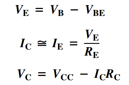
Once you know the base voltage, you can find the voltages and currents in the circuit, as follows:

Once you know VC and VE, you can determine VCE.
VCE = VC – VE
Related Articles :
Engineering Tutorial Keywords:
- Simple transistor voltage divider calculation
