In the transistor circuit analysis, it is generally required to determine the collector current for various collector-emitter voltages. One of the methods can be used to plot the output characteristics and determine the collector current at any desired collector-emitter voltage. However, a more convenient method, known as load line method can be used to solve such problems. As explained later in this section, this method is quite easy and is frequently used in the analysis of transistor applications.
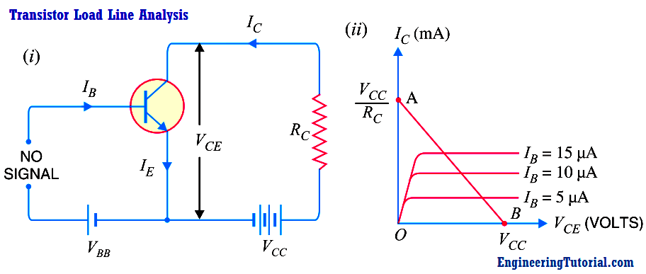
d.c. load line. Consider a common emitter npn transistor circuit shown in Fig. (i) where no signal is applied. Therefore, d.c. conditions prevail in the circuit. The output characteristics of this circuit are shown in Fig. (ii).
The value of collector-emitter voltage VCE at any time is given by ;
VCE = VCC – IC RC

As VCC and RC are fixed values, therefore, it is a first degree equation and can be represented by a straight line on the output characteristics. This is known as d.c. load line and determines the locus of VCE IC points for any given value of RC. To add load line, we need two end points of the straight line. These two points can be located as under :
(i) When the collector current IC = 0, then collector-emitter voltage is maximum and is equal to V cc i.e
Max. VCE = VCC – IC RC = VCC as (IC = 0)
This gives the first point B (OB = VCC) on the collector-emitter voltage axis as shown in Fig. (ii).
(ii) When collector-emitter voltage VCE = 0, the collector current is maximum and is equal to VCC /RC i.e.
VCE = VCC – IC RC or
0 = VCC – IC RC
Max. IC = VCC /RC
This gives the second point A (OA = VCC /RC) on the collector current axis as shown in Fig. (ii). By joining these two points, d.c. *load line AB is constructed.

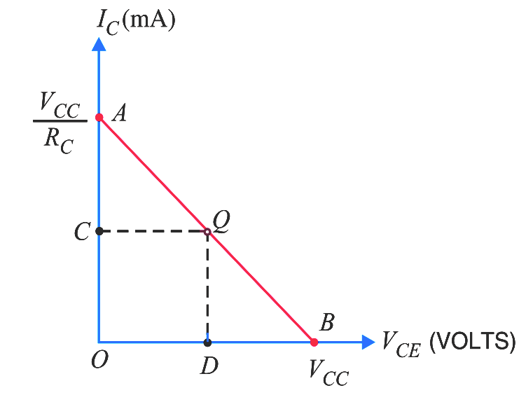
Importance. The current (IC) and voltage (VCE) conditions in the transistor circuit are represented by some point on the output characteristics. The same information can be obtained from the load line. Thus when IC is maximum (= VCC /RC), then VCE = 0 as shown in Above Fig. If IC = 0, then VCE is maximum and is equal to VCC. For any other value of collector current say OC, the collector-emitter voltage VCE = OD. It follows, therefore, that load line gives a far more convenient and direct solution to the problem.
Note. If we plot the load line on the output characteristic of the transistor, we can investigate the behaviour of the transistor amplifier. It is because we have the transistor output current and voltage specified in the form of load line equation and the transistor behaviour itself specified implicitly by the output characteristics.
Why load line ? The resistance RC connected to the device is called load or load resistance for the circuit and, therefore, the line we have just constructed is called the load line.


