The Snubber circuit is one type of dv/dt protection circuit of the thyristor.
With the help of snubber circuit, the false turn-on of a thyristor due to large dv/dt can be prevented.
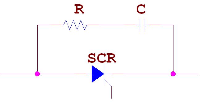 RC Snubber Circuit for SCR dv/dt Protection:
This type of snubber circuit consists of a series combination of resistance R and Capacitance C in parallel with a SCR.
- When a reverse voltage is applied, commutation process is initiated and the forward current flow through SCR approaches zero.
- Due to the inductance, current continuous to flow due to sweeping of charge carries at the external junctions.
- When it reaches a peak value it cannot be further supported by the charge carriers and falls very quickly to zero. This causes a voltage spike with the value of L(di/dt).
- Also when the supply is closed to the circuit( in the above figure say the switch S is closed), sudden voltage appears across SCR.
- Now, as the thyristor current is zero it can be considered as an open switch.
- At this moment, the capacitor C behaves like a short-circuit and therefore voltage across the SCR is zero.
- With the passage of time capacitor C gets charged at a slow rate such that dv/dt across the capacitor and therefore across SCR is less than the specified maximum dv/dt rating of the device.
- Thus the capacitor protects the SCR against high voltages and high dv/dt.
Based on the above discussion we can say that simply a Capacitor C is sufficient to protect the SCR against dv/dt false triggering.
Then what is the purpose of resistance R?
- In the RC snubber circuit, the resistance R limits the discharge current of capacitor at the instant of firing of SCR.
- Before SCR is fired, capacitor C charges to full voltage V.
- If SCR is fired, when the capacitor voltage is maximum, it discharges through the local path formed by capacitor C, Resistance R and SCR.
- During this time, if the resistance R is not included in the circuit, the discharge current will be high and consequently may damage the SCR due to large di/dt.
- Thus the Resistance R in the snubber circuit reduces the discharge current of the capacitor C and thus protect the SCR against large di/dt.
In actual practice, R, C and the load current parameters should be such that
- dv/dt across C during its charging is less than the specified dv/dt rating of the SCR
- Discharge current at the turn ON of the SCR is within reasonable limits.
Normally R,S and load circuit parameters form an undamped circuit so that dv/dt is limited to acceptable values.
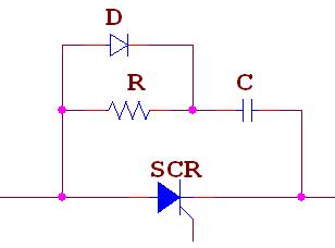
In some RC snubber circuits, a diode D used to connect in parallel with the resistor R. It is used for the purpose of bypass and thus giving improved dv/vt protection.
Related Articles :
Engineering Tutorial Keywords:
- snubber circuit
- snubber circuit basics