A transistor amplifies current because the collector current is equal to the base current multiplied by the current gain, b. The base current in a transistor is very small compared to the collector and emitter currents. Because of this, the collector current is approximately equal to the emitter current.
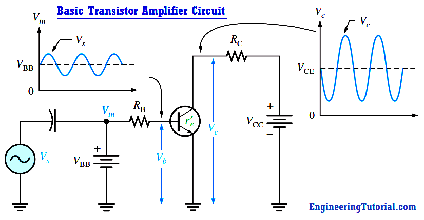
With this in mind, let’s look at the circuit in Figure. An ac voltage, Vs, is superimposed on the dc bias voltage VBB by capacitive coupling as shown. The dc bias voltage VCC is connected to the collector through the collector resistor, RC.

Fig : Basic transistor amplifier circuit with ac source voltage Vs and dc bias voltage VBB superimposed.
The ac input voltage produces an ac base current, which results in a much larger ac collector current. The ac collector current produces an ac voltage across RC, thus producing an amplified, but inverted, reproduction of the ac input voltage in the active region of operation, as illustrated in Above Figure.
The forward-biased base-emitter junction presents a very low resistance to the ac signal. This internal ac emitter resistance is designated re in Figure and appears in series with RB. The ac base voltage is
Vb = Ie.re
The ac collector voltage, Vc, equals the ac voltage drop across RC.
Vc = IcRC
Since Ic = Ie, the ac collector voltage is
Vc = IeRC
Vb can be considered the transistor ac input voltage where Vb = Vs – IbRB. Vc can be considered the transistor ac output voltage. Since voltage gain is defined as the ratio of the output voltage to the input voltage, the ratio of Vc to Vb is the ac voltage gain, Av, of the transistor.
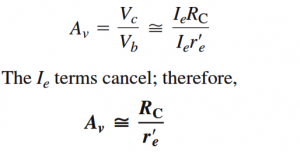
Av = Vc / Vb
Substituting IeRC for Vc and Ie.re for Vb yields

The above Equation shows that the transistor in Above Figure provides amplification in the form of voltage gain, which is dependent on the values of RC and re.
Since RC is always considerably larger in value than re , the output voltage for this configuration is greater than the input voltage.


