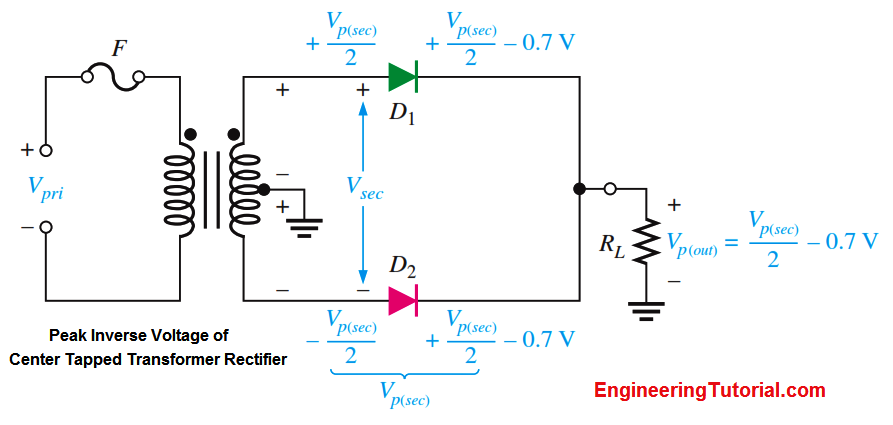
Peak Inverse Voltage Each diode in the full-wave rectifier is alternately forward-biased and then reverse-biased. The maximum reverse voltage that each diode must withstand is the peak secondary voltage Vp(sec). This is shown in Figure where D2 is assumed to be reverse-biased (red) and D1 is assumed to be forward-biased (green) to illustrate the concept.

Fig : Diode reverse voltage ( D2 Reverse Biased & D1 Forward Biased )
When the total secondary voltage Vsec has the polarity shown, the maximum anode voltage of D1 is Vp(sec)> 2 and the maximum anode voltage of D2 is -Vp(sec)>2. Since D1 is assumed to be forward-biased, its cathode is at the same voltage as its anode minus the diode drop; this is also the voltage on the cathode of D2.
The peak inverse voltage across D2 is

Therefore, by substitution, the peak inverse voltage across either diode in a full-wave center tapped rectifier is


