Two or more amplifiers can be connected in a cascaded arrangement with the output of one amplifier driving the input of the next. Each amplifier in a cascaded arrangement is known as a stage. The basic purpose of a multistage arrangement is to increase the overall voltage gain.
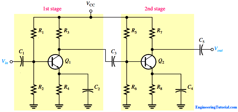
For purposes of illustration, we will use the two-stage capacitively coupled amplifier in Figure. Note that both stages are identical common-emitter amplifiers with the output of the first stage capacitively coupled to the input of the second stage. Capacitive coupling prevents the dc bias of one stage from affecting that of the other but allows the ac signal to pass without attenuation because XC = 0 ohms at the frequency of operation. Notice, also, that the transistors are labeled Q1 and Q2.

Loading Effects
In determining the voltage gain of the first stage, you must consider the loading effect of the second stage. Because the coupling capacitor C3 effectively appears as a short at the signal frequency, the total input resistance of the second stage presents an ac load to the first stage. Looking from the collector of Q1, the two biasing resistors in the second stage, R5 and R6, appear in parallel with the input resistance at the base of Q2.
In other words, the signal at the collector of Q1 “sees” R3, R5, R6, and Rin(base2) of the second stage all in parallel to ac ground. Thus, the effective ac collector resistance of Q1 is the total of all these resistances in parallel. The voltage gain of the first stage is reduced by the loading of the second stage because the effective ac collector resistance of the first stage is less than the actual value of its collector resistor, R3.


