A metal-oxide-semiconductor field-effect transistor(MOSFET) is developed by combining the areas of field-effect concept and MOS technology.
The Conventional planar MOSFET has the restriction of handling the high power. In high power applications, the Double-diffused vertical MOSFET or VMOS is used which is simply known as Power MOSFET.
What is Power MOSFET?
The Power MOSFET is the three terminal (Gate, Drain and Source), four layer (n+pn–n+),Unipolar ( only majority carriers in conduction) semiconductor device.
- The MOSFET is a majority carrier device, and as the majority carriers have no recombination delays, the MOSFET achieves extremely high bandwidths and switching times.
- The gate is electrically isolated from the source, and while this provides the MOSFET with its high input impedance, it also forms a good capacitor.
- MOSFETs do not have secondary breakdown area, their drain to source resistance has a positive temperature coefficient, so they tend to be self protective.
- It has very low ON resistance and no junction voltage drop when forward biased. These features make MOSFET an extremely attractive power supply switching device.
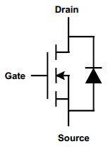
MOSFET Symbol:
The symbol for n-channel MOSFET is given below. The direction of the arrow on the lead that goes to the body region indicates the direction of current flow. As this is the symbol for n channel MOSFET, the arrow is inwards. For p-channel MOSFET, the arrow will be towards outside.

MOSFET Structure:
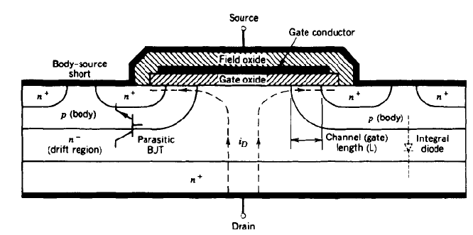
- The Power MOSFET has a vertically oriented four layer structure of alternating P and N type(n+pn–n+) layers.
- The P type middle layer is called as body of MOSFET. In this region , the channel is formed between source and drain.
- The n- layer is called as drift region,which determines the breakdown voltage of the device. This n- region is present only in Power MOSFETs not in signal level MOSFET.
- The gate terminal is isolated from body by silicon dioxide layer.
- When the positive gate voltage is applied with respect to source, the n-type channel is formed between source to drain.
- As shown in the figure, there is a parasitic npn BJT between source and drain.
- To avoid this BJT turns on, the p-type body region is shorted to source region by overlapping the source metallization on to the p type body.
- The result is a parasitic diode which is formed between drain to source terminals. This integral diode plays an important role in half and full bridge converter circuits.
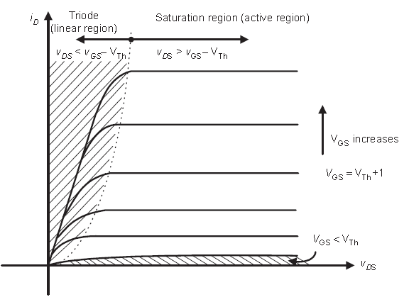
MOSFET VI Characteristics:
The VI characteristics of n-channel enhancement mode MOSFET.

Also Read: Comparison of MOSFET and BJT
