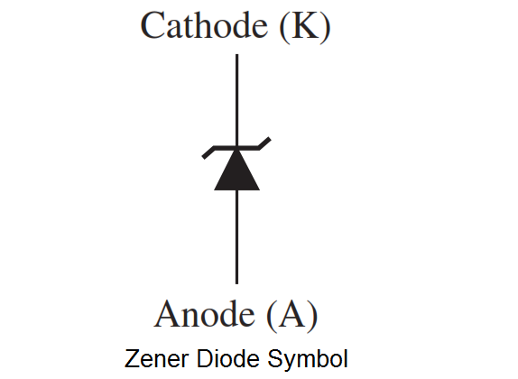
The symbol for a zener diode is shown in Below Figure. Instead of a straight line representing the cathode, the zener diode has a bent line that reminds you of the letter Z (for zener).
A zener diode is a silicon pn junction device that is designed for operation in the reverse-breakdown region. The breakdown voltage of a zener diode is set by carefully controlling the doping level during manufacture.
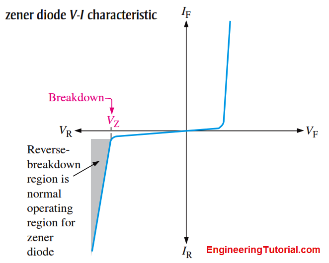
From the discussion of the diode characteristic curve in previous article, that when a diode reaches reverse breakdown, its voltage remains almost constant even though the current changes drastically, and this is the key to zener diode operation. This volt-ampere characteristic is shown again in Below Figure with the normal operating region for zener diodes shown as a shaded area.
Zener Breakdown
Zener diodes are designed to operate in reverse breakdown. Two types of reverse breakdown in a zener diode are avalanche and zener. The avalanche effect occurs in both rectifier and zener diodes at a sufficiently high reverse voltage. Zener breakdown occurs in a zener diode at low reverse voltages. A zener diode is heavily doped to reduce the breakdown voltage. This causes a very thin depletion region. As a result, an intense electric field exists within the depletion region. Near the zener breakdown voltage (V), the field is intense enough to pull electrons from their valence bands and create current.
Zener diodes with breakdown voltages of less than approximately 5 V operate predominately in zener breakdown. Those with breakdown voltages greater than approximately 5 V operate predominately in avalanche breakdown. Both types, however, are called zener diodes. Zeners are commercially available with breakdown voltages from less than 1 V to more than 250 V with specified tolerances from 1% to 20%.
Zener Breakdown Characteristics
Below Figure shows the reverse portion of a zener diode’s characteristic curve. Notice that as the reverse voltage (VR) is increased, the reverse current (IR) remains extremely small up to the “knee” of the curve. The reverse current is also called the zener current, IZ. At this point, the breakdown effect begins; the internal zener resistance, also called zener impedance (ZZ), begins to decrease as the reverse current increases rapidly. From the bottom of the knee, the zener breakdown voltage (VZ) remains essentially constant although it increases slightly as the zener current, IZ, increases.
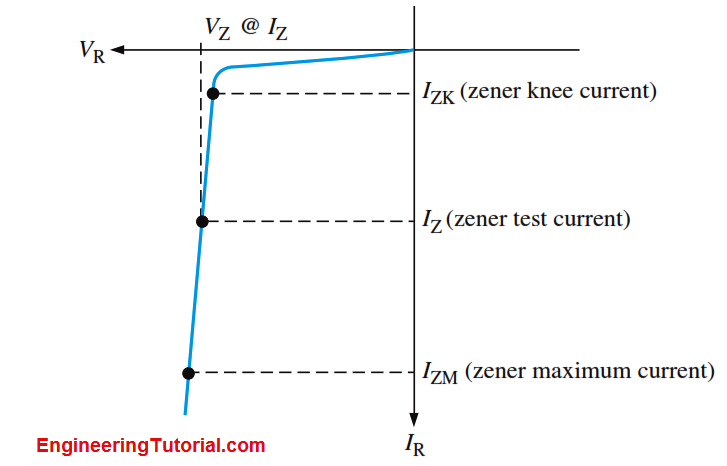
Fig : Reverse characteristic of a zener diode. VZ is usually specified at a value of the zener current known as the test current.
Zener Regulation
The ability to keep the reverse voltage across its terminals essentially constant is the key feature of the zener diode. A zener diode operating in breakdown acts as a voltage regulator because it maintains a nearly constant voltage across its terminals over a specified range of reverse-current values.
A minimum value of reverse current, IZK, must be maintained in order to keep the diode in breakdown for voltage regulation. You can see on the curve in Above Figure that when the reverse current is reduced below the knee of the curve, the voltage decreases drastically and regulation is lost. Also, there is a maximum current, IZM, above which the diode may be damaged due to excessive power dissipation. So, basically, the zener diode maintains a nearly constant voltage across its terminals for values of reverse current ranging from IZK to IZM. A nominal zener voltage, VZ, is usually specified on a datasheet at a value of reverse current called the zener test current.
Zener Equivalent Circuits
The Below Figure shows the ideal model (first approximation) of a zener diode in reverse breakdown and its ideal characteristic curve. It has a constant voltage drop equal to the nominal zener voltage. This constant voltage drop across the zener diode produced by reverse breakdown is represented by a dc voltage symbol even though the zener diode does not produce a voltage.
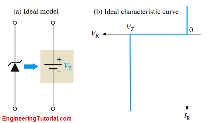
Fig : Ideal zener diode equivalent circuit model and the characteristic curve.
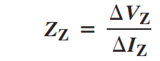
Below Figure (a) represents the practical model (second approximation) of a zener diode, where the zener impedance (resistance), ZZ, is included. Since the actual voltage curve is not ideally vertical, a change in zener current (ΔIZ) produces a small change in zener voltage (ΔVZ), as illustrated in Below Figure (b). By Ohm’s law, the ratio of ΔVZ to ΔIZ is the impedance, as expressed in the following equation:
Normally, ZZ is specified at the zener test current. In most cases, you can assume that ZZ is a small constant over the full range of zener current values and is purely resistive. It is best to avoid operating a zener diode near the knee of the curve because the impedance changes dramatically in that area.
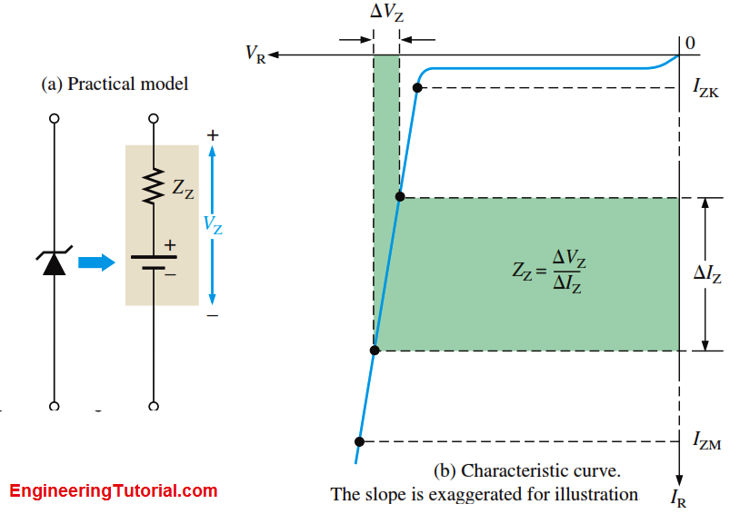
Fig : Practical zener diode equivalent circuit and the characteristic curve illustrating ZZ.
For most circuit analysis and troubleshooting work, the ideal model will give very good results and is much easier to use than more complicated models. When a zener diode is operating normally, it will be in reverse breakdown and you should observe the nominal breakdown voltage across it. Most schematics will indicate on the drawing what this voltage should be.
A major application for zener diodes is as a type of voltage regulator for providing stable reference voltages for use in power supplies, voltmeters, and other instruments.
Zener Diode Breakdown Voltage
- Zener breakdown
- Avalanche breakdown
- In various protection circuits.
- In zener limiters i.e., clipping circuits which are used to clip off the unwanted portion of the voltage waveform.
- As a voltage regulating element in voltage regulators.