Silicon diode: Use of P-doped silicon and N-doped silicon to make a P-N junction that causes the blocking effect
Schokky diode: Use of (normally) P-doped silicon bonded to metal. The junction effect is at the metal connection and it is because only one doped-tpye of silicon is used you end up with the lower on-state.
Schottky generally has lower reverse voltage max. You can easily find silicon diodes with 20-1400v ranges, while commonly schottky is 20v-60v.
Schottky is extremely fast recovery, even faster than so-called “fast recovery” silicon diodes. So you can use them in high frequency SMPS.
Forward voltage drop is lower. In silicon you get 0.6v-0.7v at rated current. In schottky you can get 0.3v which is great for SMPS.
Most schottky diodes look exactly the same is a regular diode.
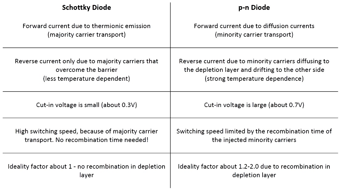
| COMPARISON OF CHARACTERISTICS OF SCHOTTKY DIODE AND PN DIODE | ||
|---|---|---|
| CHARACTERISTIC | SCHOTTKY DIODE | PN JUNCTION DIODE |
| Forward current mechanism | Majority carrier transport. | Due to diffusion currents, i.e. minority carrier transport. |
| Reverse current | Results from majority carriers that overcome the barrier. This is less temperature dependent than for standard PN junction. | Results from the minority carriers diffusing through the depletion layer. It has a strong temperature dependence. |
| Turn on voltage | Small – around 0.2 V. | Comparatively large – around 0.7 V. |
| Switching speed | Fast – as a result of the use of majority carriers because no recombination is required. | Limited by the recombination time of the injected minority carriers. |
Related Articles :
Engineering Tutorial Keywords:
- Schottky Diode
- pin diode working principle